Major contribution toward practical application of lightweight, disposable organic circuits
A research group at Yamagata University led by Shizuo Tokito, Distinguished Research Professor at the Research Center for Organic Electronics, and Ube Industries, Ltd. (president: Michio Takeshita) announced today that they have jointly developed a new n-type organic semiconductor material*1 that is soluble in organic solvents. This is the first time in the world to that a printing method has been used to manufacture high-performance n-type organic transistors with an electron mobility*2 exceeding 3cm2/Vs and stable in air. Compared to the conventional manufacturing technology that uses inorganic materials, such as silicon, the staple material currently in use today, the new technology enables the manufacture of integrated circuits (ICs) that are lighter and more flexible than ever before with lower cost.
There has never before been a report on the development of an n-type organic semiconductor that is both stable in air and has a high electron mobility of 3cm2/Vs, which exceeds the general 0.5 to 1cm2/Vs of amorphous silicon used in, for example, LCD screens, while at the same time being printable at a practical level. The development of an organic semiconductor that is soluble in organic solvents and possesses advanced electronic properties will dramatically accelerate the practical application of low-cost, flexible organic ICs manufactured using an all-printing process.
The technology for manufacturing electronic devices by printing circuits on plastic film is known as the printed electronics process, and it is already starting to be used in practical applications, such as wiring for touch panels. Moving forward, this technology is expected to be applied to semiconductor circuits, which are an even more complex type of electronic device, and development is actively underway for materials that are essential therein, including high-performance conductive ink, insulating resin, and semiconductor ink.
Semiconductors control the flow of electricity by combining p-type and n-type semiconductors, and these two types of semiconductors are used in ICs. While there have been countless reports of high-electron-mobility p-type organic semiconductors that are organic-solvent soluble and printable, there have been almost no reports of high-performance n-type organic semiconductors. This is because n-type organic semiconductors are chemically susceptible to atmospheric water and oxygen, and it has been difficult for them to maintain advanced electronic properties when used in electronic devices.
The latest joint research dramatically improved n-type organic semiconductor stability, which has been an ongoing issue, and it also enabled the development of organic semiconductors that are readily soluble in organic solvents and at the same time feature advanced electrical properties. By using this material, both p-type and n-type semiconductors will together make it possible to create organic ICs that are low in cost and use less power, and there are hopes that this will contribute to the development of new electronic devices that are wearable, mobile, and flexible.
The technology that was developed is the result of joint research that began in 2011 between Prof. Tokito's group at Yamagata University and Ube Industries, Ltd. Applicable patent applications have already been filed. By harnessing Yamagata University's expertise in material design for high-performance semiconductor materials and technology for manufacturing and evaluating printed electronic devices, along with Ube Industries' many years of expertise and technology concerning organic synthesis, the joint team was able to study the molecular design of organic semiconductors that are stable in air, soluble in solvents, and feature advanced electronic properties, as well as synthesize materials, improve purity, manufacture transistor elements, evaluate element performance, and optimize the structure of transistor elements.
The newly developed n-type organic semiconductor coating film is highly uniform and extremely thin. By optimizing coating formation conditions and the structure of transistor elements, a high electron mobility of 3cm2/Vs or more was achieved in organic transistors that were manufactured using this new semiconductor material.
With conventional n-semiconductors, there is the issue of electron mobility being easily hindered within the organic semiconductor layer by atmospheric water and oxygen. This new technology achieves great stability by conferring strong electron acceptability to all electrons in order to dramatically lower the impact water and oxygen has on electron conduction.
Work is now underway to both optimize the molecular structure of transistors and study circuit prototyping (for instance, CMOS circuits) in order to apply this technology to organic ICs. In conjunction with this, work is also underway to improve molecular structure in order for further improvements to solubility and electron mobility, aiming to obtain an organic semiconductor that is easier to use.
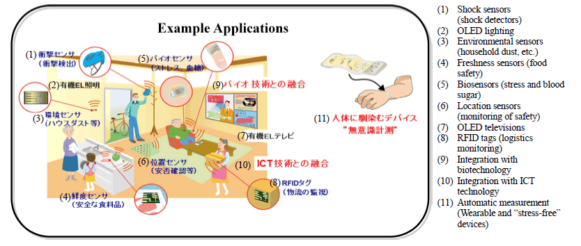
Efforts are also being made to prototype printed ICs by such means as inkjet printing that uses the newly-developed organic semiconductor, and development is moving forward, using this technology to create radio frequency ID (RFID) tags that employ organic transistors, flexible biosensors, and flexible displays.
Ube Industries, Ltd. will soon start to provide samples of the coatable n-type organic semiconductors that were developed.
In addition to these groundbreaking efforts, the transistor properties exhibited by this n-type organic semiconductor will also be announced at the Third Cross-Industry Exchange, Research Group on Electrical and Electronic Properties of Polymer and Organics, Society of Polymer Science, Japan to be held on March 14, 2014 in Yonezawa-shi, Yamagata Prefecture, and at the 61st Spring Meeting of the Japan Society of Applied Physics to be held on March 17 to 20, 2014 on the Sagamihara Campus, Aoyama Gakuin University.
Note: These results were also made possible by support from the Establishment of International Center for Advanced Organic Electronics Research, a part of the Japan Regional Innovation Strategy Program by the Excellence (J-RISE), Japan Science and Technology Agency.
The development of a printable high-performance n-type organic semiconductor is a great achievement made possible through industrial-academic collaboration in the Japan Regional Innovation Strategy Program by the Excellence (J-RISE), Japan Science and Technology Agency.
The development period stretched over nearly three years. The printable n-type organic semiconductors that have been available possessed vastly inferior properties compared to p-type organic semiconductors. By successfully creating an n-type with performance equivalent to p-types, we were able to create high-performance CMOS circuits that combine p-type and n-type organic transistors, as well as accelerate the level of integration density for organic electronic circuits, including low power consumption, and high-speed operation logic circuits and control circuits.
Using an all-printing manufacturing process that has a low environmental impact and is capable of multiproduct, small lot production at a low cost, I am confident that the newly-developed n-type semiconductor will contribute to the field of printed electronics with high-added value, including RFID tags, sensors, and flexible displays.
Ube Industries has positioned information and electronics as one of our new priority areas in our R&D portfolio. In this area, we are introducing cutting-edge technology and factoring in market needs using open innovation on our proprietary technology platform in an effect to be the first in future applications, and our joint research with Prof. Tokito's team at the Research Center for Organic Electronics, Yamagata University, is one part of that effort.
Within this joint research, the development of an n-type semiconductor that can be used in print-manufacturing of electronic devices is being viewed as a highly significant step in opening up a new field in printed electronics. This n-type organic semiconductor has the potential to become an epoch-making material that will be one key in achieving integrated circuits through printing.
Moving forward, our company is setting its sights on the challenge of aggressively engaging in this new area so that this budding technology can flower into a new business.
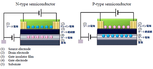
*1 An n-type semiconductor is a semiconductor made out of an organic compound, unlike conventional semiconductors made out of inorganic materials, such as silicon. Electrical current flows by the movement of the negative charges (electrons) within the n-type semiconductor. The positive charge (electron holes) is able to flow in the opposing p-type semiconductor.
*2 Electron mobility indicates the level of ease with which electrons move though a semiconductor. The higher the value, the faster the signal-switching performance will be. With LCDs, for example, using a semiconductor with high electron mobility enables the representation of smooth movement. With conventional n-type organic semiconductors, mobility of up to about 1-2.5cm2/Vs has been reported. The mobility of amorphous silicon used in general LCDs and other applications is about 0.5-1cm2/Vs.


